| CPC H10B 41/27 (2023.02) [G11C 5/06 (2013.01); H01L 29/0653 (2013.01); H10B 43/27 (2023.02)] | 17 Claims |
|
1. A semiconductor device comprising:
a substrate;
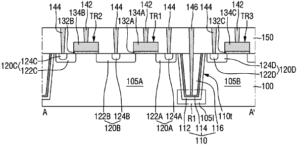
an element isolation film that defines a first active region in the substrate, the element isolation film comprising an insulating liner, an etching blocking liner on the insulating liner, and a gap fill insulating film that is on the etching blocking liner;
a first gate electrode on the first active region;
a first source/drain region located inside the first active region between the element isolation film and the first gate electrode; and
an isolation contact that extends in a vertical direction intersecting an upper face of the substrate, in the gap fill insulating film,
wherein a lower face of the isolation contact is in contact with the etching blocking liner of the element isolation film, and
wherein the isolation contact is configured to have a voltage applied thereto.
|
|
9. A semiconductor device comprising:
a substrate including an element isolation trench that defines an active region;
an element isolation film that includes an insulating liner extending along a profile of the element isolation trench, an etching blocking liner on the insulation liner, and a gap fill insulating film that is in the element isolation trench on the etching blocking liner;
a gate electrode on the active region;
a source/drain region in the active region between the element isolation film and the gate electrode; and
an isolation contact in the element isolation film, wherein the isolation contact extends in the gap fill insulating film in a vertical direction and has a lower face in contact with the etching blocking liner, the vertical direction intersecting an upper face of the substrate.
|
|
16. A nonvolatile memory device that includes a first substrate of a peripheral circuit region, and a second substrate of a cell region, the nonvolatile memory device comprising:
a first circuit element and a second circuit element on the first substrate;
an element isolation film that separates the first circuit element and the second circuit element in the first substrate, the element isolation film comprising an insulating liner, an etching blocking liner on the insulating liner, and a gap film insulating film on the etching blocking liner;
an isolation contact that extends in a vertical direction intersecting an upper face of the first substrate in the gap fill insulating film and having a lower face in contact with the etching blocking liner;
a plurality of word lines sequentially stacked on the second substrate;
a channel structure that intersects the plurality of word lines, on the second substrate; and
a bit line connected to the channel structure,
wherein the isolation contact is configured to have a voltage applied thereto.
|