| CPC H10B 12/50 (2023.02) [H10B 12/0335 (2023.02); H10B 12/09 (2023.02); H10B 12/315 (2023.02); H10B 12/34 (2023.02)] | 19 Claims |
|
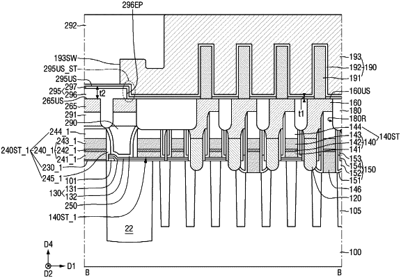
1. A semiconductor memory device, comprising:
a substrate including a cell region and a peri region around the cell region, the cell region including an active region defined by an element separation film;
a storage pad connected to the active region of the cell region; a peri gate structure on the substrate of the peri region;
a peri contact plug on both sides of the peri gate structure and electrically connectable to the substrate;
a first interlayer insulating film on the storage pad and on the peri contact plug, and including a nitride-based insulating material; and
an information storage circuit connected to the storage pad,
wherein a thickness of the first interlayer insulating film on an upper surface of the storage pad is less than a thickness of the first interlayer insulating film on an upper surface of the peri contact plug,
wherein the first interlayer insulating film is on and over the upper surface of the peri contact plug, and
wherein the first interlayer insulating film includes a lower interlayer insulating film, the lower interlayer insulating is on and over the upper surface of the peri contact plug and is not on the upper surface of the storage pad.
|