| CPC H10B 12/315 (2023.02) [H01L 23/528 (2013.01); H01L 23/53266 (2013.01); H10B 12/34 (2023.02); H10B 61/22 (2023.02); H10N 50/01 (2023.02); H10N 50/10 (2023.02); H10N 50/80 (2023.02)] | 20 Claims |
|
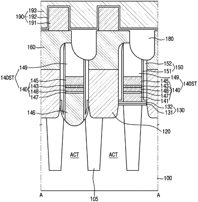
1. A semiconductor device, comprising:
a substrate including an element isolation film and an active region defined by the element isolation film;
a word line crossing the active region of the substrate in a first direction that is parallel to a top surface of the substrate; and
a bit line structure crossing the active region of the substrate in a second direction that crosses the first direction,
wherein:
the bit line structure includes:
a first conductive pattern on the active region of the substrate,
a second conductive pattern on the first conductive pattern,
a third conductive pattern on the second conductive pattern,
a fourth conductive pattern on the third conductive pattern, and
a capping pattern on the fourth conductive pattern,
the first conductive pattern of the bit line structure includes a doped semiconductor material,
the second conductive pattern of the bit line structure includes a metal silicide,
the third conductive pattern of the bit line structure includes a barrier film, and
the fourth conductive pattern of the bit line structure includes molybdenum (Mo).
|