| CPC H10B 12/31 (2023.02) [H01L 21/31144 (2013.01); H01L 21/76802 (2013.01); H01L 21/76877 (2013.01); H01L 28/75 (2013.01); H10B 12/033 (2023.02)] | 14 Claims |
|
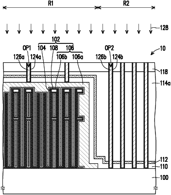
1. A semiconductor device, comprising:
a substrate comprising a memory array region and a peripheral circuit region;
a capacitor located in the memory array region and comprising:
a first electrode located on the substrate;
a second electrode located on the first electrode; and
an insulating layer located between the first electrode and the second electrode;
a stop layer comprising a first portion located on the second electrode in the memory array region and a second portion located in the peripheral circuit region, wherein the first portion extends to the second portion, a material of the stop layer is not a conductive material, and a top surface of the first portion is higher than a top surface of the second portion;
a first contact located in the memory array region, passing through the stop layer, and electrically connected to the second electrode; and
a second contact located in the peripheral circuit region and passing through the stop layer, wherein
the second electrode comprises a multilayer structure, and
the second electrode comprises:
a first conductive layer, wherein a material of the first conductive layer comprises a doped semiconductor material; and
a second conductive layer located between the first conductive layer and the insulating layer, wherein a material of the second conductive layer comprises titanium, titanium nitride, or a combination thereof.
|