| CPC H10B 12/20 (2023.02) [G11C 11/40 (2013.01); G11C 11/401 (2013.01); G11C 11/404 (2013.01); G11C 11/4096 (2013.01); H10B 12/036 (2023.02)] | 9 Claims |
|
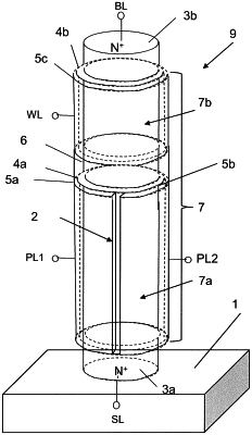
1. A semiconductor-element-including memory device comprising:
a first semiconductor base having, relative to a substrate, a central axis lying in a perpendicular direction or a horizontal direction;
a first impurity layer and a second impurity layer connecting to both ends of the first semiconductor base;
a first gate insulating layer disposed closer to the first impurity layer and surrounding a portion the first semiconductor base;
a second gate insulating layer disposed closer to the second impurity layer and surrounding the first semiconductor base between the first gate insulating layer and the second impurity layer;
a first gate conductor layer surrounding a first region in an outer periphery of the first gate insulating layer;
a second gate conductor layer, in horizontal sectional view, isolated from the first gate conductor layer and surrounding a second region, which is different from the first region, in the outer periphery of the first gate insulating layer;
a third gate conductor layer surrounding the second gate insulating layer; and
a first insulating layer disposed between the first gate conductor layer and the third gate conductor layer and between the second gate conductor layer and the third gate conductor layer,
wherein the first impurity layer, the second impurity layer, the first gate conductor layer, the second gate conductor layer, and the third gate conductor layer are disposed such that voltages applied to the first impurity layer, the second impurity layer, the first gate conductor layer, the second gate conductor layer, and the third gate conductor layer are controlled to perform a memory write operation, a memory read operation, and a memory erase operation, and
wherein the first impurity layer, the second impurity layer, the first gate conductor layer, the second gate conductor layer, and the third gate conductor layer are disposed such that voltages applied to the first impurity layer, the second impurity laver, the first gate conductor layer, the second gate conductor layer, and the third gate conductor layer are controlled to perform the memory write operation of discharging, of an electron group and a hole group generated within the first semiconductor base due to an impact ionization phenomenon caused by a current flowing between the first impurity layer and the second impurity layer or a gate induced drain leakage current, the electron group from the first semiconductor base and causing a portion of or entirety of the hole group to remain within the first semiconductor base, and the memory erase operation of discharging, from the first semiconductor base, the remaining hole group of the hole group.
|