| CPC H05K 3/188 (2013.01) [C25D 5/022 (2013.01); C25D 7/00 (2013.01); G03F 7/20 (2013.01); H05K 2203/025 (2013.01)] | 13 Claims |

|
1. A method of manufacturing a printed circuit board, the method comprising:
forming a resist layer;
exposing first areas of the resist layer spaced apart from each other;
after exposing the first areas, exposing second areas of the resist layer, the second areas being spaces between the first areas;
forming first and second openings spaced apart from each other in the first and second areas by developing the resist layer; and
forming a plurality of conductor patterns by filling the first and second openings with conductors,
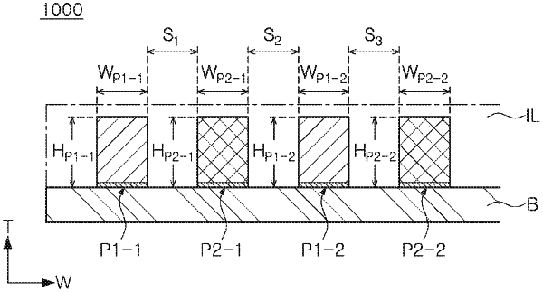
wherein the first openings include a 1-1st opening and a 1-2nd opening spaced apart from each other,
the second openings include a 2-1st opening and a 2-2nd opening spaced apart from each other,
the plurality of conductor patterns include a 1-1st conductor pattern formed in the 1-1st opening, a 1-2nd conductor pattern formed in the 1-2nd opening, a 2-1st conductor pattern formed in the 2-1st opening, and a 2-2nd conductor pattern formed in the 2-2nd opening,
when the plurality of conductor patterns are taken in cross sections thereof in a thickness direction, each of WP1-1, WP1-2, WP2-1, and WP2-2 is 0.5 μm or more and 5 μm less, where WP1-1 is an average line width of the 1-1st conductor pattern, WP2-1 is an average line width of the 2-1st conductor pattern, WP1-2 is an average line width of the 1-2nd conductor pattern, and WP2-2 is an average line width of the 2-2nd conductor pattern, and
a ratio of a width of each of spaces between the 1-1st, 2-1st, 1-2nd, and 2-2nd conductor patterns with respect to an average height of the 1-1st, 2-1st, 1-2nd, and 2-2nd conductor patterns is more than ¼ and less than ⅗.
|