| CPC H05K 1/117 (2013.01) [H01R 12/721 (2013.01); H01R 12/737 (2013.01); H05K 5/0286 (2013.01); H01R 2201/06 (2013.01); H05K 1/141 (2013.01); H05K 1/181 (2013.01); H05K 2201/094 (2013.01)] | 9 Claims |
|
1. A computing card system for an information handling system, the computing card system comprising:
a computing card, including:
a first side defined between a first edge and a second edge of the computing card, the second edge opposite to the first edge, the first side including:
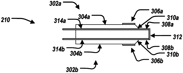
a first body surface, the first body surface including a first plurality of conductive pads connected respectively with a first set of pins of a computing card receptacle;
a first indented surface connected with a second set of pins of the computing card receptacle;
a first connecting surface defined between the first body surface and the first indented surface;
a second side defined between the first edge and the second edge of the computing card, the second side of the computing card opposite to the first side of the computing card, the second side including:
a second body surface, the second body surface including a second plurality of conductive pads connected respectively with a third set of pins of the computing card receptacle;
a second indented surface, wherein the second indented surface is conductive, the second indented surface connected with a fourth set of pins of the computing card receptacle;
a second connecting surface defined between the second body surface and the second indented surface;
a conductive bottom surface defined between the first edge and the second edge, and between the first indented surface and the second indented surface; and
a plurality of conductive internal layers, wherein a first and a second conductive internal layer of the conductive internal layers are exposed at the first indented surface and a third and a fourth conductive internal layer of the conductive internal layers are exposed at the second indented surface, wherein both the first conductive internal layer and the third conductive internal layer are connected to the conductive bottom surface and the second and the fourth conductive internal layer are not connected to the conductive bottom surface.
|