US 12,015,864 B2
Comparator, AD converter, solid-state imaging device, electronic apparatus, and method of controlling comparator
Masaki Sakakibara, Kanagawa (JP); Kenichi Aoyagi, Kanagawa (JP); and Seiji Yamada, Kanagawa (JP)
Assigned to Sony Group Corporation, Tokyo (JP)
Filed by SONY GROUP CORPORATION, Tokyo (JP)
Filed on Jul. 19, 2023, as Appl. No. 18/354,917.
Application 18/354,917 is a continuation of application No. 17/838,925, filed on Jun. 13, 2022, granted, now 11,758,305.
Application 17/838,925 is a continuation of application No. 16/999,557, filed on Aug. 21, 2020, granted, now 11,394,912, issued on Jul. 19, 2022.
Application 16/999,557 is a continuation of application No. 16/438,219, filed on Jun. 11, 2019, granted, now 10,944,932, issued on Mar. 9, 2021.
Application 16/438,219 is a continuation of application No. 15/961,584, filed on Apr. 24, 2018, granted, now 10,348,992, issued on Jul. 9, 2019.
Application 15/961,584 is a continuation of application No. 14/916,652, granted, now 10,021,331, issued on Jul. 10, 2018, previously published as PCT/JP2015/068962, filed on Jul. 1, 2015.
Claims priority of application No. 2014-144389 (JP), filed on Jul. 14, 2014.
Prior Publication US 2023/0362514 A1, Nov. 9, 2023
Int. Cl. H04N 25/77 (2023.01); H01L 27/146 (2006.01); H03K 5/24 (2006.01); H04N 25/75 (2023.01); H04N 25/772 (2023.01); H04N 25/79 (2023.01)
CPC H04N 25/77 (2023.01) [H01L 27/1461 (2013.01); H01L 27/14612 (2013.01); H01L 27/14621 (2013.01); H01L 27/14627 (2013.01); H01L 27/14634 (2013.01); H01L 27/14636 (2013.01); H01L 27/1464 (2013.01); H01L 27/14645 (2013.01); H03K 5/24 (2013.01); H03K 5/2481 (2013.01); H04N 25/75 (2023.01); H04N 25/772 (2023.01); H04N 25/79 (2023.01)] 20 Claims
OG exemplary drawing
 
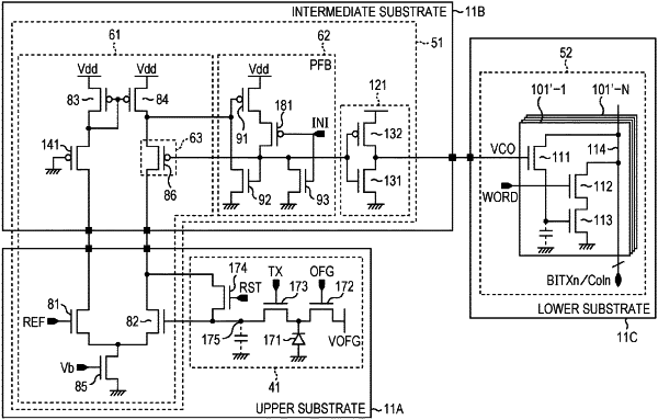
1. A light detecting device, comprising:
a first substrate;
a second substrate laminated to the first substrate; and
a third substrate laminated to the second substrate,
wherein:
the first substrate includes:
a pixel circuit having a photodiode, and
a first part of a differential amplification circuit coupled to the pixel circuit,
the second substrate includes a second part of the differential amplification circuit coupled to the first part of the differential amplification circuit, and
the third substrate includes a latch storage unit coupled to the second part of the differential amplification circuit.