| CPC H04N 25/767 (2023.01) [H04N 25/75 (2023.01)] | 15 Claims |

|
1. An imaging circuit comprising:
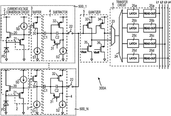
a plurality of circuit blocks each including a photoelectric conversion element configured to photoelectrically convert incident light to generate a photocurrent, and a current-voltage conversion circuit configured to convert the photocurrent into a voltage signal;
a quantizer configured to generate a detection signal of an address event in accordance with a result of comparing the voltage signal supplied from at least one of the plurality of circuit blocks with a threshold;
a demultiplexer connected to a subsequent stage of the quantizer; and
a plurality of latch circuits connected to different output terminals of the demultiplexer, wherein
the number of the latch circuits is equal to or larger than two and equal to or smaller than twice the number of the photoelectric conversion elements.
|