| CPC H04L 27/36 (2013.01) [H03K 17/687 (2013.01); H03K 19/096 (2013.01); H03K 19/21 (2013.01); H04L 25/40 (2013.01)] | 20 Claims |

|
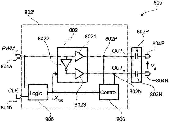
1. A circuit, comprising:
a first input node configured to receive a pulse-width modulated input signal;
a second input node configured to receive a clock signal having a frequency higher than a frequency of said pulse-width modulated input signal;
a logic circuit sensitive to said clock signal and configured to generate a control signal as a function of said clock signal, wherein said control signal is normally set to a first logic value, and is periodically set to a second logic value for a transmission time interval in response to an edge being detected in said clock signal, said transmission time interval being shorter than a half clock period of said clock signal;
a tri-state transmitter coupled to the first input node to receive said pulse-width modulated input signal and sensitive to said control signal, the tri-state transmitter being configured to produce a first output signal at a first transmitter output node and a second output signal at a second transmitter output node, the first output signal and the second output signal having a voltage swing between a positive supply voltage and a reference supply voltage; and
an output control circuit sensitive to said control signal and coupled to said first transmitter output node and said second transmitter output node,
wherein:
in response to said control signal having said first logic value, said tri-state transmitter sets said first transmitter output node and said second transmitter output node to a high impedance state, and said output control circuit drives said first transmitter output node and said second transmitter output node to an intermediate voltage level between said positive supply voltage and said reference supply voltage; and
in response to said control signal having said second logic value, said tri-state transmitter drives said first transmitter output node to said positive supply voltage or to said reference supply voltage according to the logic value of said pulse-width modulated input signal, and drives said second transmitter output node to said positive supply voltage or to said reference supply voltage according to an inverted logic value of said pulse-width modulated input signal,
wherein said tri-state transmitter is faster than said output control circuit in driving said first transmitter output node and said second transmitter output node.
|