| CPC H03M 1/08 (2013.01) | 20 Claims |
|
1. A noise filtering circuit comprising:
a first amplifier configured to receive a bias voltage at a first input terminal, receive a bias output voltage through a feedback path at a second input terminal, and compensate for a difference between the bias voltage and the bias output voltage;
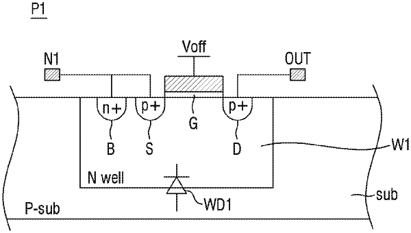
a first transistor connected to an output of the first amplifier and having a gate terminal to which an off-voltage is applied;
a first capacitor connected to the first transistor;
a second capacitor connected to the output of the first amplifier;
a second transistor connected to the second capacitor and having a gate terminal to which an off-voltage is applied; and
a second amplifier having a first input terminal connected to the first capacitor and a second input terminal connected to the second transistor.
|