|
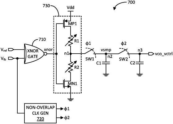
1. An apparatus, comprising: a phase lock loop (PLL), comprising: a phase detector and loop pass filter (PD/LF), comprising: a phase/frequency detector including a first input configured to receive a reference signal, and a second input configured to receive a feedback signal, and an output configured to produce an output signal based on the reference and feedback signals; a first capacitor; a charge pump, comprising: a charging path configured to generate a charging current to charge the first capacitor based on the output signal, wherein the charging path comprises a first field effect transistor (FET) coupled between an upper voltage rail and a first node; and a discharging path including a first resistor configured to discharge the first capacitor, wherein the discharging path comprises the first resistor and a second FET coupled in series between the first node and a lower voltage rail, wherein gates of the first and second FETs are coupled to the output of the phase/frequency detector and a first switching device coupled between the first node and a second node, wherein the first capacitor is coupled between the second node and the lower voltage rail.
|