| CPC H03K 3/356191 (2013.01) [H03K 3/012 (2013.01); H03K 3/013 (2013.01); H03K 3/356121 (2013.01)] | 22 Claims |
|
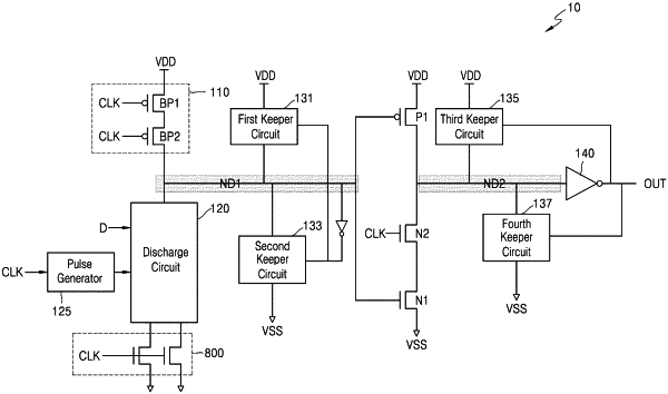
1. A flip flop comprising:
a precharge circuit configured to charge a first node by bridging a power voltage node and the first node according to a voltage level of a clock signal, the pre-charge circuit including at least two PMOS transistors arranged directly in series, the at least two PMOS transistors configured to simultaneously receive a same clock signal;
a discharge circuit configured to discharge the first node by bridging the first node and a ground node according to an input signal and the clock signal;
a second node configured to be charged or discharged according to a voltage level of the first node; and
an additional discharge circuit between the discharge circuit and the ground node includes at least two NMOS transistors arranged in parallel, the at least two NMOS transistors configured to simultaneously receive the same clock signal.
|