| CPC H03K 3/35613 (2013.01) [H03K 19/0008 (2013.01); H03K 19/00361 (2013.01); H03K 19/0175 (2013.01); H03K 19/018528 (2013.01)] | 20 Claims |
|
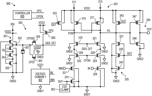
1. A circuit comprising:
a level shifter including an input to receive a signal in a first voltage domain and an output to provide a level shifted signal of the signal in a second voltage domain, the level shifter including a shift path between a first node and a second node, the shift path including a third node for conveying a state of the signal, the shift path including a first transistor and a second transistor coupled in series in the shift path, wherein the second transistor includes a control terminal to receive a low power signal to place the second transistor in a non-conductive state during a low power mode of the level shifter;
a GIDL detection circuit including an output to provide a GIDL signal indicative of a GIDL current condition where the GIDL signal increases the conductivity of the first transistor when the GIDL signal is indicative of the GIDL current condition to minimize a GIDL current through at least a portion of the shift path when the second transistor is nonconductive during the low power mode of the level shifter.
|