| CPC H03K 19/1733 (2013.01) | 13 Claims |

|
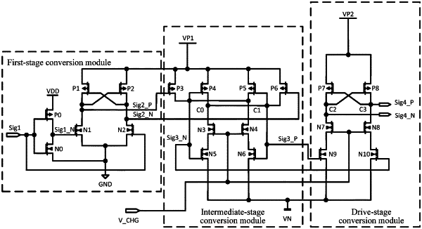
1. A logic process-based level conversion circuit of a flash field programmable gate array (FPGA) comprising a first-stage conversion module, an intermediate-stage conversion module, and a drive-stage conversion module, wherein the first-stage conversion module, the intermediate-stage conversion module, and the drive-stage conversion module are successively cascaded, wherein
the first-stage conversion module is configured to convert an input first signal of a VDD-GND voltage domain into a second signal of a VP1-GND voltage domain and output the second signal to the intermediate-stage conversion module; the intermediate-stage conversion module is configured to convert the input second signal of the VP1-GND voltage domain into a third signal of a VP1-VN voltage domain and output the third signal to the drive-stage conversion module; and the drive-stage conversion module is configured to convert the input third signal of the VP1-VN voltage domain into a drive signal of a VP2-VN voltage domain and output a word line for driving the flash FPGA; and
a logic process is controlled to output a corresponding voltage combination to complete an erasure operation or a programming operation on the flash FPGA, wherein the voltage combination comprises a core low voltage VDD, an intermediate voltage VP1, a drive-stage voltage VP2, and a negative voltage VN, wherein the core low voltage VDD, the intermediate voltage VP1, the drive-stage voltage VP2, and the negative voltage VN are provided by the logic process, wherein GND is a grounding voltage and VP2≥VP1≥VDD.
|