| CPC H02M 3/07 (2013.01) [G05F 1/468 (2013.01); G05F 1/565 (2013.01); G05F 1/575 (2013.01); H02M 1/0045 (2021.05)] | 10 Claims |
|
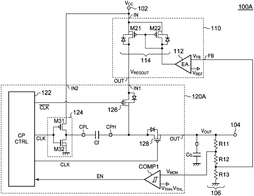
1. A power supply circuit comprising:
an input terminal to be connected to receive an input voltage;
an output terminal to be connected to a load;
a linear regulator having an input node connected to the input terminal, and an output node, and structured to adjust an intermediate voltage at the output node such that an output voltage at the output terminal approaches a first target voltage; and
a Dixon-type charge pump circuit having a first input node connected to receive the intermediate voltage, a second input node connected to receive the input voltage, and an output node connected to the output terminal,
wherein the charge pump circuit is structured to enter a disable state when the output voltage is higher than a threshold voltage determined to be lower than the first target voltage, to output a voltage at the first input node to the output node in the disable state, to enter an enable state when the output voltage is lower than the threshold voltage, and to stabilize the output voltage to a second target voltage determined to be lower than the first target voltage in the enable state.
|