| CPC H01S 5/18308 (2013.01) [H01S 5/04252 (2019.08); H01S 5/18369 (2013.01); H01S 5/18377 (2013.01); H01S 5/209 (2013.01)] | 19 Claims |
|
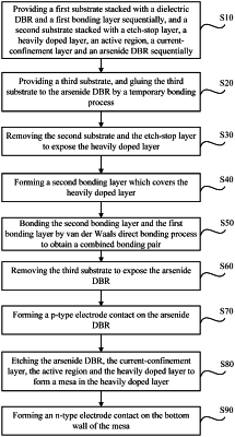
1. A method of fabricating vertical cavity surface emitting laser, comprising:
providing a first substrate stacked with a dielectric distributed Bragg reflector (DBR) and a first bonding layer sequentially, and a second substrate stacked with a etch-stop layer, a heavily doped layer, an active region, a current-confinement layer and an arsenide DBR sequentially;
providing a third substrate, and gluing the third substrate to the arsenide DBR by a temporary bonding process;
removing the second substrate and the etch-stop layer to expose the heavily doped layer;
forming a second bonding layer which covers the heavily doped layer;
bonding the second bonding layer and the first bonding layer by van der Waals direct bonding process to obtain a combined bonding pair;
removing the third substrate to expose the arsenide DBR;
forming a p-type electrode contact on the arsenide DBR;
etching the arsenide DBR, the current-confinement layer, the active region and the heavily doped layer to form a mesa in the heavily doped layer;
forming an n-type electrode contact on the bottom wall of the mesa.
|