| CPC H01S 5/06203 (2013.01) [H01S 5/0427 (2013.01); H01S 5/12 (2013.01); H04B 10/40 (2013.01)] | 9 Claims |
|
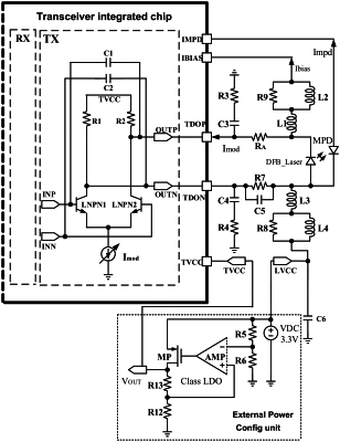
1. A DFB laser DC-coupled output power configuration scheme with adjustable voltage difference, characterized in that, said power configuration scheme comprising: an external power configuration unit for providing two electric DC power supplies with a fixed voltage difference for a DFB laser and a transmitting unit TX of an optical transceiver integrated chip, said external power configuration unit comprises a DC voltage source VDC3.3V and a LDO-like (low dropout-like) stabilizer, and said LDO-like stabilizer comprises a resistor R5, a resistor R6, a resistor R12, a resistor R13, a PMOS power resistor MP and an operational amplifier AMP;
one end of the resistor R6 is simultaneously connected to one end of the resistor R5 and the inverting input terminal of the operational amplifier AMP;
a non-inverting input terminal of the operational amplifier AMP is simultaneously connected to one end of the resistor R12 and one end of the resistor R13;
another end of the resistor R13 is simultaneously connected to a drain end of a PMOS power transistor MP and a voltage output port VOUT, and the voltage output port VOUT is arranged to output a working power of the transmitting unit TX of the optical transceiver integrated chip, the voltage output port VOUT is connected to a power supply voltage port TVCC of the transmitting unit TX;
a gate end of the PMOS power transistor MP is connected to an output terminal of the operational amplifier AMP;
a source end of the PMOS power resistor MP and another end of the resistor R5 are connected to a positive terminal of the DC voltage source VDC;
another end of the resistor R12, another end of the resistor R6 and a negative terminal of the DC voltage source VDC are connected to the ground;
said power configuration scheme optimizes said transmitting unit TX at the same time, an optimization scheme to optimize said transmitting unit TX is that: said transmitting unit TX comprises transistors which are all low-voltage high-speed tubes, and said transmitting unit TX comprises a negative capacitance structure composed of capacitors C1 and C2 serving as an auxiliary structure for improving bandwidth;
a minimum voltage of said power supply voltage port TVCC of said transmitting unit TX is 2.7V after optimization.
|