| CPC H01L 33/62 (2013.01) [H01L 33/382 (2013.01); H01L 33/46 (2013.01); H01L 33/486 (2013.01); H01L 33/50 (2013.01); H01L 33/60 (2013.01); H01L 33/405 (2013.01); H01L 33/641 (2013.01)] | 19 Claims |

|
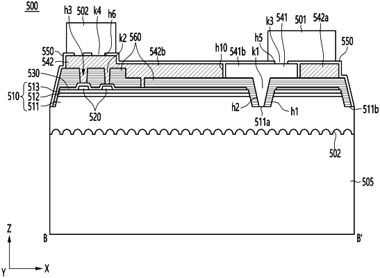
1. A light emitting device package comprising:
a substrate;
a light emitting structure including a first conductive type semiconductor layer disposed on the substrate, an active layer disposed on the first conductive type semiconductor layer, and a second conductive type semiconductor layer disposed on the active layer;
a first electrode disposed on the light emitting structure and electrically connected to the first conductive type semiconductor layer;
a second electrode disposed on the light emitting structure and electrically connected to the second conductive type semiconductor layer;
a protective layer disposed on the first and second electrodes and insulating between the first and second electrodes;
a first and second frames disposed to be spaced apart from each other;
a body disposed surrounding the first and second frames and having first and second openings spaced apart from each other;
a light emitting device disposed on the body and including first and second bonding portions; and
first and second conductive portions disposed in the first and second openings, respectively,
wherein the first and second openings vertically overlap the first and second frames, respectively,
the first and second conductive portions are electrically connected to the first and second frames, respectively,
the first and second bonding portions are disposed in the first and second openings, respectively, and are electrically connected to the first and second conductive portions,
the light emitting device includes a support region disposed on the body outside the first and second openings,
the first bonding portion is disposed on the first electrode and electrically connected to the first electrode, and the second bonding portion is disposed on the second electrode and electrically connected to the second electrode,
the protective layer includes one or a plurality of first open regions exposing a part of an upper surface of the first electrode and one or a plurality of second open regions exposing a part of an upper surface of the second electrode,
the first bonding portion is electrically connected to a part of the upper surface of the first electrode exposed through the first open region, and
the second bonding portion is electrically connected to a part of the upper surface of the second electrode exposed through the second open region.
|