| CPC H01L 33/60 (2013.01) [H01L 33/46 (2013.01); H01L 33/486 (2013.01); H01L 33/50 (2013.01); H01L 33/505 (2013.01); H01L 33/56 (2013.01); H01L 2933/0033 (2013.01); H01L 2933/0041 (2013.01); H01L 2933/0058 (2013.01)] | 19 Claims |

|
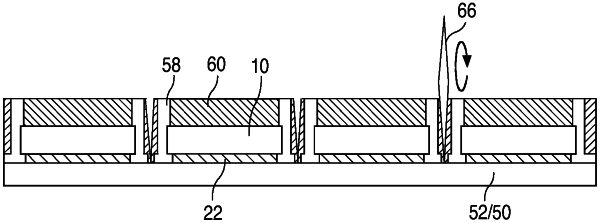
1. A light-emitting diode (LED) device comprising:
a semiconductor structure comprising a top surface, a bottom surface opposite the top surface, and a plurality of side surfaces;
a wavelength-converting structure over the top surface of the semiconductor structure, the wavelength-converting structure having a top surface, a bottom surface opposite the top surface, and a plurality of side surfaces;
at least two electrodes electrically coupled to the semiconductor structure via the bottom surface of the semiconductor structure;
a reflective layer completely encasing the plurality of side surfaces of both the semiconductor structure and the wavelength-converting structure and extending to the top surface of the wavelength-converting structure, wherein the reflective layer has a top surface, a bottom surface opposite the top surface, and a plurality of side surfaces; and
a protective layer encasing the side surfaces of the reflective layer.
|