| CPC H01L 29/78642 (2013.01) [H01L 21/02178 (2013.01); H01L 21/02488 (2013.01); H01L 21/02568 (2013.01); H01L 29/24 (2013.01); H01L 29/66969 (2013.01); H01L 29/78645 (2013.01); H01L 29/78696 (2013.01); H10B 99/00 (2023.02); H01L 21/0262 (2013.01)] | 19 Claims |
|
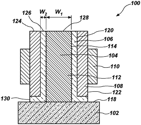
1. A transistor, comprising:
a channel comprising a two-dimensional material directly laterally adjacent to a seed material, the channel oriented perpendicular to a base material, a width of the seed material laterally adjacent to the channel greater than a width of the channel;
a gate dielectric directly adjacent to the two-dimensional material on a side of the channel opposite the seed material, a horizontally-oriented portion of the two-dimensional material vertically underling the gate dielectric, and an outer sidewall of the gate dielectric and an outermost lateral edge of the horizontally-oriented portion of the channel substantially vertically aligned with one another; and
a gate adjacent to the gate dielectric.
|