US 12,015,088 B2
Display device and method of fabricating the same
Sang Sub Kim, Suwon-si (KR); Keun Woo Kim, Seongnam-si (KR); Ji Yeong Shin, Suwon-si (KR); Yong Su Lee, Seoul (KR); Myoung Geun Cha, Seoul (KR); Ki Seok Choi, Seoul (KR); and Sang Gun Choi, Suwon-si (KR)
Assigned to SAMSUNG DISPLAY CO., LTD., Yongin-si (KR)
Filed by Samsung Display Co., LTD., Yongin-si (KR)
Filed on Mar. 17, 2023, as Appl. No. 18/122,815.
Application 18/122,815 is a division of application No. 17/071,579, filed on Oct. 15, 2020, granted, now 11,626,429.
Claims priority of application No. 10-2019-0149743 (KR), filed on Nov. 20, 2019.
Prior Publication US 2023/0223478 A1, Jul. 13, 2023
Int. Cl. H01L 29/786 (2006.01); H01L 27/12 (2006.01); H01L 29/66 (2006.01); H10K 59/121 (2023.01); G09G 3/32 (2016.01); H01L 21/225 (2006.01); H01L 21/265 (2006.01); H01L 21/28 (2006.01); H10K 59/12 (2023.01)
CPC H01L 29/78603 (2013.01) [H01L 27/1274 (2013.01); H01L 29/6675 (2013.01); H10K 59/1213 (2023.02); G09G 3/32 (2013.01); G09G 2300/0809 (2013.01); H01L 21/2253 (2013.01); H01L 21/26533 (2013.01); H01L 21/28158 (2013.01); H01L 27/1255 (2013.01); H10K 59/1201 (2023.02)] 11 Claims
OG exemplary drawing
 
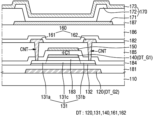
1. A method of fabricating a display device, the method comprising:
forming a buffer layer on a surface of a substrate:
forming an amorphous silicon pattern on the buffer layer;
implanting oxygen into a lower portion of the amorphous silicon pattern; and
dividing the amorphous silicon pattern into which the oxygen is implanted into a lower gate insulating film and an active layer disposed above the lower gate insulating film, the active layer including crystalline silicon, wherein
an oxygen content of the lower gate insulating film is higher than an oxygen content of the buffer layer.