| CPC H01L 29/7853 (2013.01) [H01L 21/02532 (2013.01); H01L 21/30604 (2013.01); H01L 21/3083 (2013.01); H01L 21/823412 (2013.01); H01L 21/823431 (2013.01); H01L 27/0886 (2013.01); H01L 27/0924 (2013.01); H01L 27/1211 (2013.01); H01L 29/0657 (2013.01); H01L 29/0847 (2013.01); H01L 29/1037 (2013.01); H01L 29/16 (2013.01); H01L 29/165 (2013.01); H01L 29/41791 (2013.01); H01L 29/4966 (2013.01); H01L 29/513 (2013.01); H01L 29/518 (2013.01); H01L 29/66545 (2013.01); H01L 29/6656 (2013.01); H01L 29/66636 (2013.01); H01L 29/66772 (2013.01); H01L 29/66795 (2013.01); H01L 29/6681 (2013.01); H01L 29/66818 (2013.01); H01L 29/785 (2013.01); H01L 29/7851 (2013.01); H01L 29/7854 (2013.01); H01L 29/7856 (2013.01); H01L 29/786 (2013.01); H10B 12/056 (2023.02); H10B 12/36 (2023.02); H01L 2924/13067 (2013.01)] | 17 Claims |
|
1. A semiconductor device, comprising:
a semiconductor body above a substrate;
a gate electrode stack over a portion of the semiconductor body to define a channel region in the semiconductor body under the gate electrode stack, a first source or drain region in the semiconductor body at a first side of the gate electrode stack, and a second source or drain region in the semiconductor body at a second side of the gate electrode stack, the second side opposite the first side;
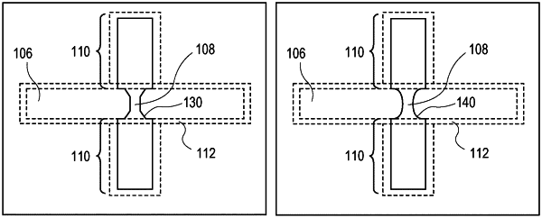
a first sidewall spacer adjacent to the first side of the gate electrode stack and over the first source or drain region, the first source or drain region having a width adjacent to the channel region and beneath the first sidewall spacer, the width greater than a width of the channel region of the semiconductor body, wherein the width of the first source or drain region is approximately 6-40% greater than the width of the channel region; and
a second sidewall spacer adjacent to the second side of the gate electrode stack and over the second source or drain region.
|