US 12,015,086 B2
Semiconductor device with a fin-shaped active region and a gate electrode
Jae-Hoon Lee, Suwon-si (KR); Gi-gwan Park, Hwaseong-si (KR); and Tae-young Kim, Hwaseong-si (KR)
Assigned to Samsung Electronics Co., Ltd., Gyeonggi-do (KR)
Filed by Samsung Electronics Co., Ltd., Suwon-si (KR)
Filed on May 10, 2021, as Appl. No. 17/315,818.
Application 17/315,818 is a continuation of application No. 16/416,725, filed on May 20, 2019, granted, now 11,038,062.
Application 16/416,725 is a continuation of application No. 15/404,697, filed on Jan. 12, 2017, granted, now 10,361,309, issued on Jul. 23, 2019.
Claims priority of application No. 10-2016-0008037 (KR), filed on Jan. 22, 2016.
Prior Publication US 2021/0265503 A1, Aug. 26, 2021
Int. Cl. H01L 29/78 (2006.01); H01L 29/08 (2006.01); H01L 29/15 (2006.01); H01L 29/16 (2006.01); H01L 29/20 (2006.01); H01L 29/22 (2006.01); H01L 29/267 (2006.01); H01L 29/66 (2006.01)
CPC H01L 29/7851 (2013.01) [H01L 29/0847 (2013.01); H01L 29/155 (2013.01); H01L 29/1608 (2013.01); H01L 29/20 (2013.01); H01L 29/2006 (2013.01); H01L 29/2206 (2013.01); H01L 29/267 (2013.01); H01L 29/66795 (2013.01); H01L 29/7848 (2013.01); H01L 29/785 (2013.01); H01L 29/7854 (2013.01)] 11 Claims
OG exemplary drawing
 
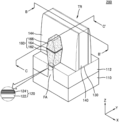
1. A semiconductor device comprising:
a substrate including a fin-shaped active region that protrudes from the substrate, the fin-shaped active region including silicon germanium;
a gate electrode on a top surface and both side walls of the fin-shaped active region;
one pair of source/drain regions on the fin-shaped active region; and
a buffer layer between the fin-shaped active region and the source/drain regions, the buffer layer including a compound semiconductor material.