| CPC H01L 29/785 (2013.01) [H01L 21/823431 (2013.01); H01L 29/0649 (2013.01); H01L 29/41791 (2013.01); H01L 29/66795 (2013.01); H01L 2029/7858 (2013.01)] | 20 Claims |

|
1. A method of manufacturing a semiconductor device, comprising:
forming a fin structure protruding from an isolation insulating layer disposed over a substrate;
forming a sacrificial gate dielectric layer over the fin structure;
forming a polysilicon layer over the sacrificial gate dielectric layer;
forming a mask pattern over the polysilicon layer;
patterning the polysilicon layer into a sacrificial gate electrode using the mask pattern as an etching mask; and
replacing the sacrificial gate dielectric layer and the sacrificial gate electrode with a metal gate structure including a high-k dielectric layer and a metal gate electrode, wherein:
the patterning the poly silicon layer includes:
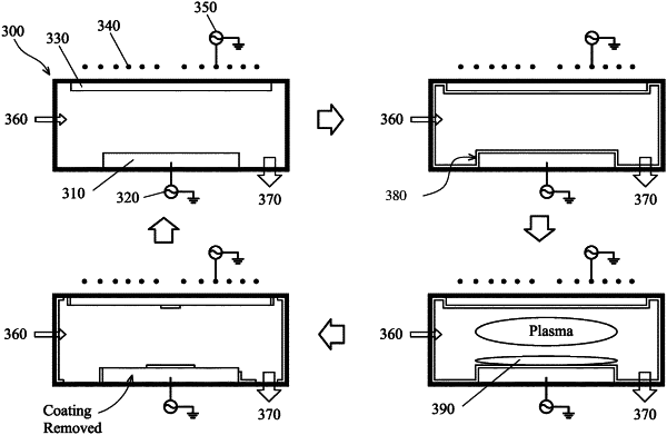
forming a coating material layer on an inner wall of an etching chamber;
loading the substrate with the polysilicon layer into the etching chamber; and
etching the polysilicon layer by plasma dry etching,
one or more etching conditions of the polysilicon etching are adjusted so that the metal gate structure has:
a first width W1 at a first level H1 from an upper surface of the isolation insulating layer, and
a second width W2 at a second level H2 from the upper surface of the isolation insulating layer,
the first level corresponds to a level of a top of the fin structure,
H2 equal to 0.45 H1, and
the first width W1 is different from the second width W2.
|