| CPC H01L 29/785 (2013.01) [H01L 29/0649 (2013.01); H01L 29/0847 (2013.01); H01L 29/6653 (2013.01); H01L 29/66795 (2013.01)] | 20 Claims |

|
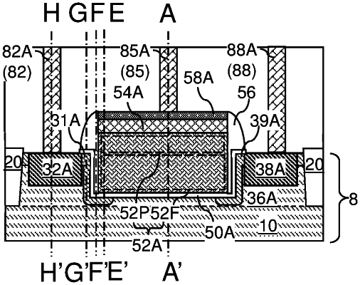
1. A field effect transistor, comprising:
at least one line trench extending downward from a top surface of a first transistor active region located in a substrate, and laterally extending along a first horizontal direction;
a gate dielectric contacting a bottom surface and sidewalls of each of the at least one line trench and comprising a planar gate dielectric portion overlying the substrate, at least one bottom gate dielectric portion contacting a bottom surface of a respective one of the at least one line trench, and vertically-extending gate dielectric portions contacting sidewalls of the at least one line trench and connecting the planar gate dielectric portion and a respective one of the at least one bottom gate dielectric portion;
a gate electrode comprising a planar gate electrode portion that overlies the planar gate dielectric portion and at least one gate electrode fin portion located within the at least one line trench;
a dielectric gate spacer laterally surrounding the gate electrode and comprising at least one pair of downward-protruding portions vertically extending into the at least one line trench, wherein each downward-protruding portion of the dielectric gate spacer comprises a respective bottom surface that contacts a top surface segment of a respective bottom gate dielectric portion of the gate dielectric; and
a source extension region in contact with end segments of a bottom surface and sidewalls of the at least one line trench and contacting a bottom surface of the planar gate dielectric portion.
|