| CPC H01L 29/785 (2013.01) [H01L 27/0924 (2013.01); H01L 29/0673 (2013.01); H01L 29/1054 (2013.01); H01L 29/1606 (2013.01); H01L 29/66795 (2013.01); H10B 12/36 (2023.02)] | 20 Claims |
|
1. A device comprising:
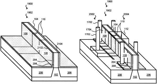
a fin disposed on a substrate, the fin including a first sidewall and an opposing second sidewall and a top surface extending between the first and second sidewalls;
a dielectric isolation structure disposed on the substrate adjacent the fin, the dielectric isolation structure having a top surface facing away from the substrate;
a two-dimensional material layer disposed directly on the first and second sidewalls of the fin without being disposed on the top surface of the fin, wherein a first channel region is defined in the two-dimensional material layer, wherein the two-dimensional material layer includes a first portion disposed directly on the top surface of the dielectric isolation structure and extending laterally away from the fin, wherein the first portion of the two-dimensional material layer has a bottom surface facing and physically contacting the top surface of the dielectric isolation structure and an opposing top surface that faces away from the top surface of the dielectric isolation structure; and
a gate stack disposed on the fin, the gate stack including a gate dielectric layer and a gate electrode layer, the gate dielectric layer physically contacting the first channel region of the two-dimensional material layer and the top surface of the fin, wherein the gate stack includes a first portion extending laterally away from the fin such that the first portion of the gate stack is disposed directly over the first portion of the two-dimensional material layer and the top surface of the dielectric isolation structure, the gate dielectric layer of the first portion of the gate stack having a bottom surface facing and physically contacting the top surface of the dielectric isolation structure and the top surface of the first portion of the two-dimensional material layer.
|