| CPC H01L 29/7838 (2013.01) [H01L 29/105 (2013.01); H01L 29/42356 (2013.01); H01L 29/66484 (2013.01); H01L 29/66492 (2013.01); H01L 29/7832 (2013.01); H01L 29/7835 (2013.01); H01L 31/1136 (2013.01); H01L 21/26513 (2013.01); H01L 21/26586 (2013.01)] | 7 Claims |
|
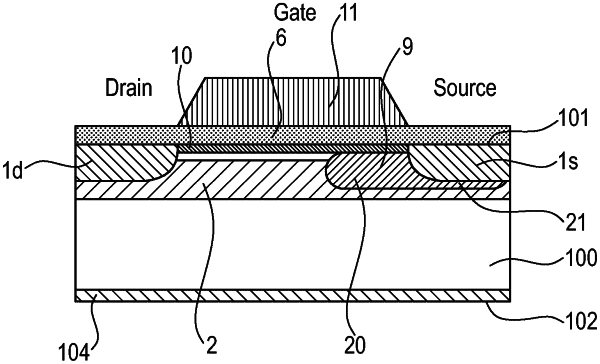
1. A DEPFET transistor comprising:
a semiconductor substrate of a first conductivity type having a first main surface and a second main surface that are opposite to each other,
a field effect transistor portion formed at the first main surface which field effect transistor portion comprises a source connection region of a second conductivity type, a drain connection region of a second conductivity type, a channel region arranged between the source connection region and the drain connection region and a gate electrode above the channel region that is separated from the channel region by a gate insulator,
a back side control region of a second conductivity type formed at the second main surface and
a substrate doping enhancement region of a first conductivity type formed at the first main surface at least under the source connection region and under the channel region,
wherein the substrate doping enhancement region comprises a signal charge control region of the first conductivity type below the gate electrode, in which the effective doping dose has a higher value than at other positions of the substrate doping enhancement region below the gate electrode, so that the extension of the signal charge control region between the source connection region and the drain connection region is smaller than the extension of the gate electrode thereabove between the source connection region and the drain connection region.
|