| CPC H01L 29/7827 (2013.01) [H01L 29/0847 (2013.01); H01L 29/1037 (2013.01); H01L 29/24 (2013.01); H01L 29/41741 (2013.01); H01L 29/45 (2013.01); H10B 12/05 (2023.02); H10B 12/31 (2023.02)] | 15 Claims |

|
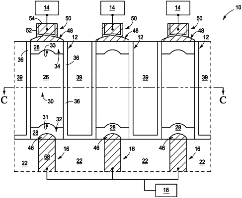
1. An integrated assembly comprising an access device between a storage element and a conductive structure; the access device comprising:
channel material comprising semiconductor material; the channel material having a first end and an opposing second end, and having a side extending from the first end to the second end; the first end being adjacent the conductive structure, and the second end being adjacent the storage element; the semiconductor material comprising at least one element selected from Group 13 of the periodic table in combination with at least one element selected from Group 16 of the periodic table;
conductive gate material adjacent the side of the channel material; and
at least one of a first domed metal-containing cap over the conductive structure and under the channel material and a second domed metal-containing cap over the channel material and under the storage element.
|