| CPC H01L 29/66734 (2013.01) [H01L 21/3083 (2013.01); H01L 29/401 (2013.01); H01L 29/407 (2013.01); H01L 29/66719 (2013.01); H01L 29/7813 (2013.01)] | 9 Claims |
|
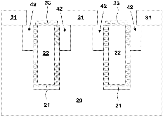
1. A manufacturing method of a semiconductor power device, comprising:
forming a first insulating layer on an n-type substrate and etching the first insulating layer to form an opening;
forming an insulating sidewall in the opening;
etching the n-type substrate using the first insulating layer and the insulating sidewall as a mask to form a first groove in the n-type substrate;
forming a second insulating layer and a shield gate in the first groove;
forming a third insulating layer on a surface of the shield gate;
etching off the insulating sidewall; and etching the n-type substrate using the first insulating layer, the second insulating layer, and the third insulating layer as a mask to form a second groove in the n-type substrate.
|