| CPC H01L 29/516 (2013.01) [C01G 23/006 (2013.01); C01G 35/006 (2013.01); H10B 51/00 (2023.02); H10B 53/00 (2023.02); C01P 2002/34 (2013.01); C01P 2002/52 (2013.01); C01P 2002/77 (2013.01); C01P 2006/40 (2013.01)] | 18 Claims |
|
1. A memory device comprising:
a dielectric material layer; and
first and second metal layers on both sides of the dielectric material layer,
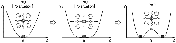
wherein the dielectric material layer comprising a compound expressed by ABO3, wherein at least one of A and B in ABO3 is substituted and doped with another atom having a larger atom radius, and ABO3 becomes A1-xA′xB1-yB′yO3 through substitution and doping, where x>0, y>=0, and a dopant A′ has an atom radius greater than A and/or a dopant B′ has an atom radius greater than B,
wherein a dielectric material property of the dielectric material layer varies according to a type of a substituted and doped dopant and a substitution doping concentration, and
wherein A is Sr, B is Ti,
A′ is any one selected from Cs, Rb, and K, and
B′ is any one selected from Zr, Hf, Sn, Nb, and Ta.
|