US 12,015,071 B2
Air spacers around contact plugs and method forming same
Chen-Huang Huang, Hsinchu (TW); Ming-Jhe Sie, Taipei (TW); Yih-Ann Lin, Jhudong Township (TW); An Chyi Wei, Hsinchu (TW); and Ryan Chia-Jen Chen, Hsinchu (TW)
Assigned to TAIWAN SEMICONDUCTOR MANUFACTURING COMPANY, LTD., Hsinchu (TW)
Filed by Taiwan Semiconductor Manufacturing Co., Ltd., Hsinchu (TW)
Filed on Jun. 6, 2022, as Appl. No. 17/805,552.
Application 17/805,552 is a continuation of application No. 16/806,280, filed on Mar. 2, 2020, granted, now 11,355,616.
Claims priority of provisional application 62/928,746, filed on Oct. 31, 2019.
Prior Publication US 2022/0310820 A1, Sep. 29, 2022
This patent is subject to a terminal disclaimer.
Int. Cl. H01L 29/49 (2006.01); H01L 21/285 (2006.01); H01L 21/3213 (2006.01); H01L 21/764 (2006.01); H01L 21/768 (2006.01); H01L 21/8234 (2006.01); H01L 29/45 (2006.01); H01L 29/66 (2006.01); H01L 29/78 (2006.01)
CPC H01L 29/4991 (2013.01) [H01L 21/28518 (2013.01); H01L 21/764 (2013.01); H01L 29/45 (2013.01); H01L 29/66795 (2013.01); H01L 29/7851 (2013.01)] 20 Claims
OG exemplary drawing
 
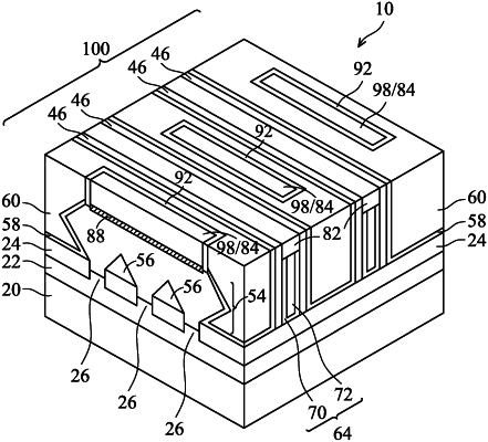
9. A device comprising:
a gate stack;
a source/drain region on a side of the gate stack;
a silicide region over the source/drain region;
a contact plug over the silicide region;
a dielectric isolation layer forming a ring encircling the contact plug; and
an air spacer, wherein in a top view of the device, the air spacer comprises a first portion forming a full ring encircling the contact plug, and wherein a top surface of the source/drain region is exposed to the air spacer.