| CPC H01L 29/42376 (2013.01) [H01L 21/823431 (2013.01); H01L 21/823456 (2013.01); H01L 27/0886 (2013.01); H01L 29/66545 (2013.01)] | 16 Claims |
|
1. A semiconductor device, comprising:
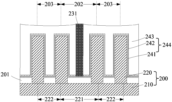
a base substrate, the base substrate including a substrate and a plurality of fins discrete from each other on the substrate;
a gate structure on the base substrate, wherein the gate structure includes a first portion in a first region and a second portion in a second region, and a length of the first portion of the gate structure in the first region is larger than a length of the second portion of the gate structure in the second region; and
a plurality of stop layers on the base substrate and located in the first portion of the gate structure in the first region, the plurality of stop layers being made of a material including SiCBN;
wherein:
the gate structure includes a gate dielectric layer on top surfaces and sidewalls of the plurality of fins, a work function layer on the gate dielectric layer, and a gate electrode layer on the work function layer; and
the gate dielectric layer is in contact with a bottom surface of the plurality of stop layers, the work function layer and the gate electrode layer are in contact with sidewall surfaces of the plurality of stop layers.
|