| CPC H01L 29/41791 (2013.01) [H01L 21/823431 (2013.01); H01L 21/823475 (2013.01); H01L 27/0886 (2013.01); H01L 29/7851 (2013.01)] | 20 Claims |
|
1. A method of manufacturing an integrated circuit device, the method comprising:
preparing a substrate having a device active region;
forming a fin-type active region, the fin-type active region protruding from the substrate on the device active region;
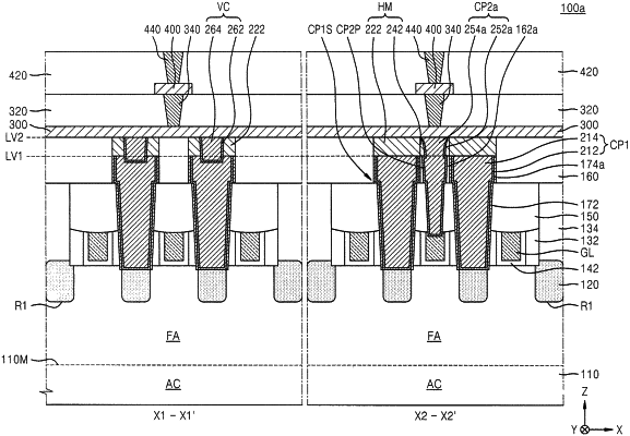
forming a gate line and source/drain regions, the gate line intersecting the fin-type active region, and the source/drain regions being located on the fin-type active region at sides of the gate line;
forming a gate insulating capping layer covering a top surface of the gate line;
forming an upper insulating layer covering the gate insulating capping layer;
forming a pair of first contact holes passing through the upper insulating layer and exposing the source/drain regions;
forming a pair of first conductive plugs filling lower portions of the pair of first contact holes, the pair of first conductive plugs being respectively connected to the source/drain regions;
forming a hard mask layer covering a top surface of each first conductive plug of the pair of first conductive plugs;
forming a second contact hole exposing the gate line by removing portions of the upper insulating layer and the gate insulating capping layer; and
forming a second conductive plug filling the second contact hole,
wherein the hard mask layer covers the top surface of each first conductive plug from a first edge of the top surface to a second edge of the top surface in a first direction, and protrudes from the top surface beyond the second edge for each first conductive plug of the pair of first conductive plugs and extends toward the second conductive plug so that a portion of the hard mask layer overhangs outside of an edge of the top surface of each first conductive plug of the pair of first conductive plugs.
|