| CPC H01L 29/0619 (2013.01) [H01L 21/26513 (2013.01); H01L 21/761 (2013.01); H01L 29/66234 (2013.01); H01L 29/73 (2013.01)] | 22 Claims |
|
1. An integrated circuit comprising:
active semiconductor devices in a substrate; and
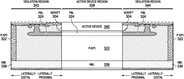
a lateral isolation region configured to isolate a given active semiconductor device from neighboring active semiconductor devices, the lateral isolation region comprising:
first and second doped regions having a first conductivity type located adjacent to a surface of the lateral isolation region, the second doped region located laterally further away from the given active semiconductor device than the first doped region;
a third doped region located laterally between the first and second doped regions and adjacent to the surface of the lateral isolation region, the third doped region having a second conductivity type opposite of the first conductivity type, the first, third, and second doped regions respectively forming a collector, a base, and an emitter of a parasitic bipolar junction transistor of the lateral isolation region; and
first and second false collector regions of the first conductivity type adjacent to the surface of the lateral isolation region, the first false collector region located laterally between the collector and the base, and the second false collector region located laterally between the base and the emitter.
|