| CPC H01L 27/156 (2013.01) [H01L 33/382 (2013.01); H01L 33/505 (2013.01); H01L 33/62 (2013.01)] | 20 Claims |

|
1. A display device comprising:
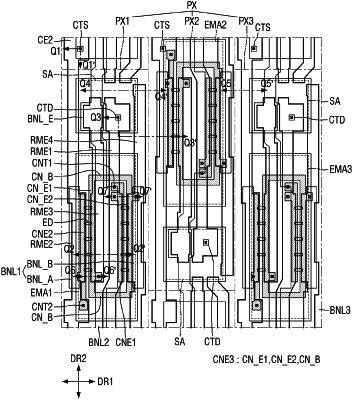
a plurality of pixels comprising a plurality of subpixels and disposed in a first direction and a second direction intersecting the first direction;
a plurality of electrodes spaced apart from each other in the first direction, extending in the second direction, and disposed in each of the plurality of subpixels;
a plurality of light emitting elements disposed in each of the plurality of subpixels and disposed on the plurality of electrodes; and
a plurality of contact electrodes electrically contacting the plurality of light emitting elements and the plurality of electrodes, wherein
each of the plurality of subpixels comprises:
an emission area comprising the plurality of light emitting elements; and
a sub area spaced apart from the emission area in the second direction, each of the plurality of pixels comprises:
a first subpixel comprising a first emission area and a sub area disposed on a first side of the first emission area in the second direction; and
a second subpixel disposed on a first side of the first subpixel in the first direction and comprises a second emission area and a sub area disposed on a second side of the second emission area in the second direction, and
the sub area of the second subpixel is disposed side by side with the first emission area in the first direction, wherein the plurality of electrodes comprise:
a first electrode disposed across the emission area and the sub area of each subpixel of the plurality of pixels;
a second electrode spaced apart from the electrode in the first direction and disposed across the plurality of subpixels;
a third electrode disposed between the first electrode and the second electrode disposed across the emission area and sub area of the plurality of subpixel; and
a fourth electrode spaced apart from the third electrode in the first direction with the first electrode interposed between the fourth electrode and the third electrode, wherein
the first electrode comprises a first electrode contact part disposed in the sub area of the plurality of subpixels, and
the second comprises a plurality of second electrode contact parts disposed at boundaries of adjacent plurality of pixels in the second direction.
|