| CPC H01L 27/14623 (2013.01) [H01L 27/14614 (2013.01); H01L 27/14621 (2013.01); H01L 27/14627 (2013.01); H01L 27/1464 (2013.01); H01L 27/14645 (2013.01); H01L 27/14685 (2013.01); H01L 27/14689 (2013.01)] | 8 Claims |
|
1. A solid-state imaging unit, comprising:
a light receiving surface; and
two or more pixels disposed to oppose the light receiving surface, wherein the two or more pixels each include:
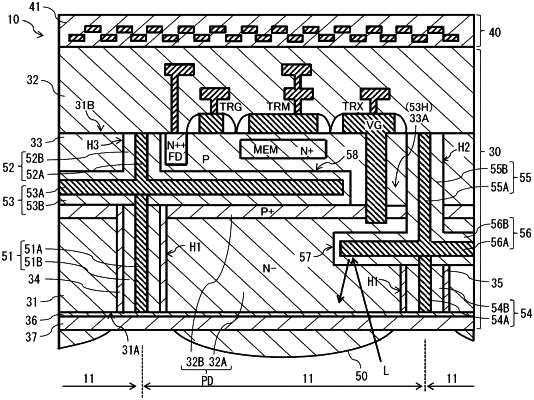
a photoelectric conversion section that performs photoelectric conversion on light having entered via the light receiving surface;
a charge holding section that holds a charge transferred from the photoelectric conversion section;
a transfer transistor that includes a vertical gate electrode reaching the photoelectric conversion section, the transfer transistor transferring the charge from the photoelectric conversion section to the charge holding section; and
two or more light-blocking sections disposed in layers that are provided between the light receiving surface and the charge holding section and are different from each other,
wherein the two or more light-blocking sections are provided at positions at which the two or more light-blocking sections do not block entry, into the photoelectric conversion section, of the light having entered via the light receiving surface and at which the two or more light-blocking sections do not provide a gap when viewed from the light receiving surface, and
wherein the two or more light-blocking sections include:
a first light-blocking section disposed in a layer between the photoelectric conversion section and the charge holding section, the first light-blocking section having an opening which the vertical gate electrode runs through, the first light-blocking section blocking, at a part other than the opening, entry, into the charge holding section, of the light having entered via the light receiving surface, and
a second light-blocking section disposed at a position that is in a layer between the light receiving surface and the first light-blocking section and opposes at least the opening, the second light-blocking section blocking the entry, into the charge holding section, of the light having entered via the light receiving surface.
|