| CPC H01L 27/14623 (2013.01) [H01L 21/02274 (2013.01); H01L 27/1462 (2013.01); H01L 27/1464 (2013.01); H01L 27/14645 (2013.01); H01L 27/14665 (2013.01); H01L 31/02162 (2013.01); H04N 25/76 (2023.01); H10K 30/88 (2023.02); H01L 27/14638 (2013.01); H10K 39/32 (2023.02)] | 11 Claims |

|
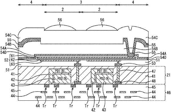
1. A solid-state imaging device, comprising:
a semiconductor substrate;
a photoelectric conversion film on an upper side of the semiconductor substrate;
a first sealing film above the photoelectric conversion film;
a second sealing film above the first sealing film, wherein the second sealing film includes a first layer and a second layer;
a third sealing film between the first sealing film and the second sealing film, wherein
the first layer of the second sealing film is under the third sealing film,
the second layer of the second sealing film is on the third sealing film,
the first layer of the second sealing film covers an entire lower surface of the third sealing film,
the second layer of the second sealing film covers an entire upper surface of the third sealing film,
the first layer of the second sealing film is on the first sealing film, and
the first layer of the second sealing film is thinner than the second layer of the second sealing film; and
a light shielding film between the first sealing film and the first layer of the second sealing film, wherein
the light shielding film is on the first sealing film, and
each of the first layer of the second sealing film, the second layer of the second sealing film, and the third sealing film is on the light shielding film.
|