| CPC H01L 27/1462 (2013.01) [H01L 27/14621 (2013.01); H01L 27/14623 (2013.01); H01L 27/1463 (2013.01); H01L 27/14645 (2013.01); H01L 27/14627 (2013.01); H01L 27/14636 (2013.01)] | 20 Claims |
|
1. A light detecting device comprising:
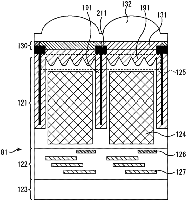
a semiconductor substrate including a first photoelectric conversion region and a first surface of a light incident side of the semiconductor substrate, wherein the first surface includes a moth-eye structure, the moth-eye structure including:
a first portion including a first angled portion in a cross-sectional view;
a second portion including a first radius of curvature in the cross-sectional view;
a third portion including a second angled portion in the cross-sectional view; and
a fourth portion including a second radius of curvature in the cross-sectional view,
wherein the moth-eye structure is disposed above the first photoelectric conversion region in the cross-sectional view,
wherein the first portion, the second portion, the third portion, and the fourth portion are disposed along at least part of the moth-eye structure in this order in the cross-sectional view,
wherein the second portion and the fourth portion are more curved than the first portion and the third portion,
wherein the second portion comprises a first part of the first surface of the semiconductor substrate that is continually curved between a first point on a first sidewall of the second portion and a second point on a second sidewall of the second portion across from the first sidewall of the second portion, and
wherein the fourth portion comprises a second part of the first surface of the semiconductor substrate that is continually curved between a first point on a first sidewall of the fourth portion and a second point on a second sidewall of the fourth portion across from the first sidewall of the fourth portion.
|