| CPC H01L 27/14603 (2013.01) [G01N 23/083 (2013.01); H01L 22/12 (2013.01)] | 17 Claims |

|
1. An X-ray pulse detection system, comprising:
a semiconductor chip comprising a bulk material;
a first plurality of drift cathode strips on a first side of the semiconductor chip;
a second plurality of drift cathode strips on a second side of the semiconductor chip, wherein each of the first plurality and the second plurality of drift cathode strips are doped with a p-type dopant;
a plurality of readout anodes positioned on the first side, wherein each of the plurality of readout anodes is doped with an n-type dopant; and
a counter cathode positioned on the second side,
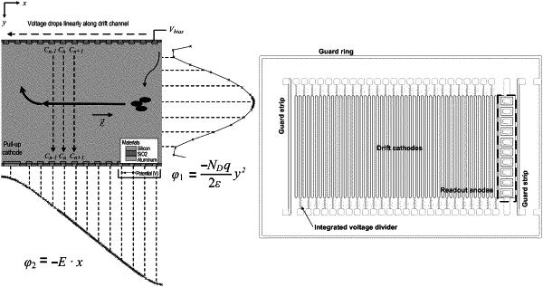
wherein the first plurality and the second plurality of drift cathode strips are configured to create a potential well in a middle section of the semiconductor chip and cause an electron cloud, generated by an X-ray pulse being incident on the semiconductor chip, to drift in a first direction towards the middle section of the semiconductor chip,
wherein the first and the second plurality of drift cathodes are configured to further create a linearly graded potential along a length of the semiconductor chip and to cause the electron cloud to drift in a second direction that is substantially perpendicular to the first direction,
wherein the plurality of readout anodes are configured to collect the electron cloud after its spreading in the middle section of the semiconductor chip, and
wherein values for a thickness of the semiconductor chip, a number of the first plurality and the second plurality of drift cathode strips, and a bias voltage applied to the first and the second plurality of drift cathode strips are selected to obtain a predetermined temporal resolution for X-ray pulses within a particular range of energies, wherein a value for the thickness of the semiconductor chip is selected from a range spanning 0.01 μm to 1000 μm, wherein a value of the number of the first plurality and the second plurality of drift cathode strips is selected from a range spanning 1 to 50, wherein a value for the bias voltage is selected from a range spanning 0V to 12V, and wherein the particular range of energies spans 1 keV to 1000 keV.
|