| CPC H01L 27/1262 (2013.01) [G02F 1/133345 (2013.01); G02F 1/1357 (2021.01); G02F 1/1676 (2019.01); H01L 27/124 (2013.01); H01L 33/005 (2013.01)] | 14 Claims |

|
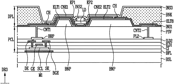
1. A method of manufacturing a display device including an emission area and a non-emission area, wherein the non-emission area includes a first area and a second area, the method comprising:
forming an uncut electrode on a substrate, wherein at least a portion of the uncut electrode is formed in the non-emission area;
disposing a first insulating laver to overlap the uncut electrode;
removing at least a portion of the first insulating layer in the non-emission area, wherein the removing of the at least a portion of the first insulating layer includes:
removing the first insulating layer disposed in the first area; and
removing the first insulating layer disposed in the second area;
cutting the at least a portion of the uncut electrode in the non-emission area;
disposing light emitting elements including a first light emitting element and a second light emitting element, wherein the first light emitting element is disposed in the emission area and the second light emitting element is disposed in an open area, and the disposing of the light emitting elements is performed after the removing of the first insulating layer disposed in the second area; and
disposing a second insulating laver to overlap the emission area and the non-emission area wherein the second light emitting element is disposed where the uncut electrode is not disposed.
|