| CPC H01L 27/0266 (2013.01) [G11C 16/22 (2013.01); H01L 21/28035 (2013.01); H01L 21/28158 (2013.01); H01L 21/3212 (2013.01); H01L 21/823456 (2013.01); H01L 21/823462 (2013.01); H01L 21/823475 (2013.01); H01L 29/0649 (2013.01); H10B 41/40 (2023.02); H10B 43/40 (2023.02); G11C 16/0483 (2013.01); G11C 16/10 (2013.01); G11C 16/14 (2013.01); G11C 16/26 (2013.01); H01L 21/31116 (2013.01); H01L 21/32137 (2013.01)] | 20 Claims |
|
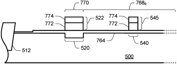
1. A method of forming a circuit-protection device, comprising:
forming a dielectric having a first thickness, and having a second thickness greater than the first thickness, over a semiconductor;
after forming the dielectric having the first thickness and having the second thickness, forming a conductor over and in contact with the dielectric having the first thickness and having the second thickness; and
patterning the conductor to retain a portion of the conductor over a portion of the dielectric having the second thickness, and to retain substantially no portion of the conductor over a portion of the dielectric having the first thickness;
wherein the retained portion of the conductor defines a control gate of a field-effect transistor of the circuit-protection device.
|