| CPC H01L 27/0222 (2013.01) [G05F 3/205 (2013.01); G05F 3/26 (2013.01); H01L 27/0928 (2013.01); H02M 3/073 (2013.01); H02M 3/078 (2021.05); H10B 12/50 (2023.02)] | 17 Claims |

|
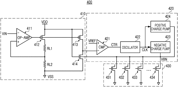
1. A body bias voltage generating circuit comprising:
a current mirror circuit configured to generate and input a target current to a target semiconductor element, the target semiconductor element being in a turned-on state; and
a charge pump circuit including an oscillator configured to output a clock signal based on a result of comparing an output voltage of the target semiconductor element with a reference voltage, and at least one charge pump configured to output a body bias voltage to each of a plurality of semiconductor elements,
wherein each of the plurality of semiconductor elements has a same conductivity type as the target semiconductor element,
the at least one charge pump includes at least one negative charge pump and at least one positive charge pump, and
the oscillator is configured to output the clock signal to the negative charge pump or the positive charge pump.
|