| CPC H01L 25/50 (2013.01) [H01L 21/4803 (2013.01); H01L 21/4853 (2013.01); H01L 23/24 (2013.01); H01L 23/3128 (2013.01); H01L 23/49827 (2013.01); H01L 25/0652 (2013.01); H01L 25/0655 (2013.01); H01L 25/18 (2013.01); H01L 24/11 (2013.01); H01L 24/13 (2013.01); H01L 24/16 (2013.01); H01L 24/29 (2013.01); H01L 24/32 (2013.01); H01L 24/73 (2013.01); H01L 24/81 (2013.01); H01L 24/92 (2013.01); H01L 24/97 (2013.01); H01L 2224/0401 (2013.01); H01L 2224/1144 (2013.01); H01L 2224/1145 (2013.01); H01L 2224/11462 (2013.01); H01L 2224/11464 (2013.01); H01L 2224/16145 (2013.01); H01L 2224/16227 (2013.01); H01L 2224/16235 (2013.01); H01L 2224/17181 (2013.01); H01L 2224/32145 (2013.01); H01L 2224/32225 (2013.01); H01L 2224/73204 (2013.01); H01L 2224/73253 (2013.01); H01L 2224/81191 (2013.01); H01L 2224/81815 (2013.01); H01L 2224/92125 (2013.01); H01L 2224/92225 (2013.01); H01L 2224/97 (2013.01); H01L 2225/06513 (2013.01); H01L 2225/06517 (2013.01); H01L 2225/06541 (2013.01); H01L 2924/14 (2013.01); H01L 2924/1431 (2013.01); H01L 2924/1432 (2013.01); H01L 2924/1434 (2013.01); H01L 2924/1461 (2013.01); H01L 2924/15311 (2013.01); H01L 2924/18161 (2013.01)] | 20 Claims |

|
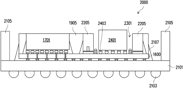
1. A package comprising:
a substrate;
a first integrated circuit die bonded to a first side of the substrate;
an annular structure bonded to the first side of the substrate adjacent the first integrated circuit die, wherein the first integrated circuit die is outside an outermost perimeter of the annular structure;
an encapsulant over the substrate and surrounding the annular structure and the first integrated circuit die, a topmost surface of the encapsulant being level with a topmost surface of the annular structure and a topmost surface of the first integrated circuit die; and
a functional component within the annular structure and bonded to the first side of the substrate, wherein the annular structure is between the encapsulant and the functional component.
|