| CPC H01L 25/167 (2013.01) [H01L 27/1248 (2013.01); H01L 33/507 (2013.01); H01L 33/56 (2013.01); H01L 33/58 (2013.01); H01L 33/641 (2013.01); H01L 2933/0041 (2013.01); H01L 2933/005 (2013.01); H01L 2933/0058 (2013.01)] | 17 Claims |

|
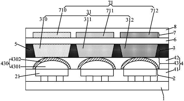
1. A display panel, comprising a substrate, and a light emitting element array and a quantum dot color filter array on the substrate, the quantum dot color filter array is arranged on a light exiting side of the light emitting element array, and quantum dot color filters in the quantum dot color filter array correspond to light emitting elements in the light emitting element array one to one,
the display panel further comprises a blocking structure arranged between the light emitting element array and the quantum dot color filter array so as to prevent heat dissipated by the light emitting elements from being conducted to the quantum dot color filters,
wherein the blocking structure comprises a first planarization layer and a second planarization layer, the first planarization layer and the second planarization layer are sequentially stacked on the substrate along a light exiting direction of the light emitting element array, and the second planarization layer is located on a side of the light emitting element array away from the substrate,
the light emitting element array is embedded in the first planarization layer, and a surface of the first planarization layer away from the substrate is flushed with a surface at the light exiting side of the light emitting element array away from the substrate.
|