| CPC H01L 25/0657 (2013.01) [H01L 23/041 (2013.01); H01L 23/3128 (2013.01); H01L 23/5383 (2013.01); H01L 24/16 (2013.01); H01L 24/17 (2013.01); H01L 24/32 (2013.01); H01L 24/73 (2013.01); H01L 2224/0401 (2013.01); H01L 2224/16227 (2013.01); H01L 2224/1703 (2013.01); H01L 2224/32145 (2013.01); H01L 2224/73203 (2013.01); H01L 2225/06562 (2013.01)] | 17 Claims |

|
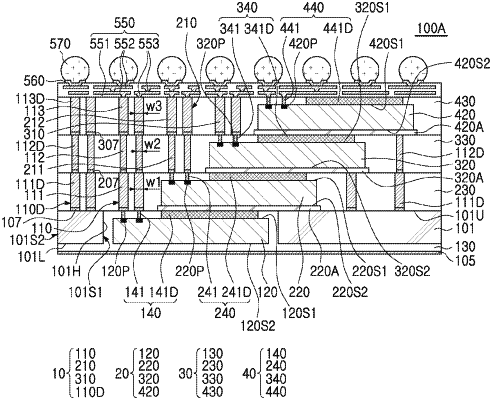
1. A semiconductor package, comprising:
a plurality of semiconductor chips comprising a first semiconductor chip having a first active surface on which first connection pads are disposed and a first inactive surface opposing the first active surface, and a second semiconductor chip disposed on the first semiconductor chip and having a second active surface on which second connection pads are disposed and a second inactive surface opposing the second active surface,
a first adhesive layer disposed below the second inactive surface of the second semiconductor chip;
first bumps disposed directly on the first connection pads;
second bumps disposed directly on the second connection pads;
at least one first dummy bump directly on the first active surface of the first semiconductor chip and spaced apart from the first bumps;
a first filling layer covering the first active surface of the first semiconductor chip, side surfaces of the first bumps, and side surfaces of the at least one first dummy bump; and
at least one second dummy bump directly on the second active surface of the second semiconductor chip and spaced apart from the second bumps,
wherein the first bump does not overlap the second semiconductor chip in a vertical direction perpendicular to an upper surface of the first semiconductor chip, and
wherein the first adhesive layer is in contact with the second semiconductor chip, the first filling layer, and the at least one first dummy bump.
|