| CPC H01L 25/0657 (2013.01) [G11C 5/063 (2013.01); H01L 29/78693 (2013.01); H10B 12/315 (2023.02); H10B 12/50 (2023.02); H01L 24/16 (2013.01); H01L 25/0655 (2013.01); H01L 2224/16145 (2013.01); H01L 2224/16225 (2013.01); H01L 2225/06513 (2013.01); H01L 2225/06517 (2013.01); H01L 2225/06541 (2013.01); H01L 2924/1431 (2013.01); H01L 2924/1436 (2013.01)] | 7 Claims |
|
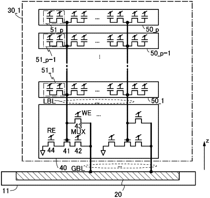
1. A semiconductor device comprising:
a silicon substrate including a first circuit;
a first element layer over the silicon substrate; and
a second element layer over the first element layer,
wherein the first element layer includes a second circuit,
wherein the second element layer includes a third circuit,
wherein the first circuit includes a driver circuit,
wherein the driver circuit includes a first transistor,
wherein the second circuit includes a second transistor,
wherein the third circuit includes a memory cell,
wherein the memory cell includes a third transistor and a first capacitor,
wherein a plurality of stacked blocks are stacked and provided in a direction perpendicular or substantially perpendicular to a surface of the silicon substrate, the stacked blocks being constituted by the first element layer and the second element layer,
wherein the driver circuit included in the first circuit and the plurality of stacked blocks overlap with each other,
wherein each of the plurality of stacked blocks includes a first wiring provided in the direction perpendicular or substantially perpendicular to the surface of the silicon substrate,
wherein the first wiring is provided in a hole penetrating the first element layer and the second element layer, and
wherein the first wirings of the plurality of stacked blocks are electrically connected to each other.
|