| CPC H01L 24/32 (2013.01) [H01L 25/0657 (2013.01); H01L 24/73 (2013.01); H01L 25/18 (2013.01); H01L 2224/32057 (2013.01); H01L 2224/32058 (2013.01); H01L 2224/32145 (2013.01); H01L 2224/73204 (2013.01); H01L 2225/06513 (2013.01); H01L 2924/10156 (2013.01)] | 20 Claims |

|
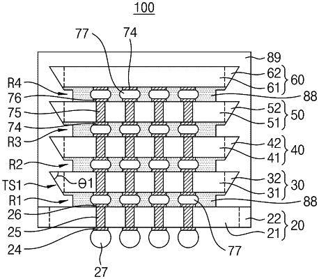
1. A semiconductor package, comprising:
a substrate;
a semiconductor chip on the substrate, the semiconductor chip including
an active region, and
a scribe lane in continuity with an edge of the active region; and
a non-conductive film (NCF) between the substrate and the semiconductor chip, the non-conductive film (NCF) at least partially defining a recess region,
wherein the recess region overlaps with the scribe lane in plan view, and extends onto the active region.
|