| CPC H01L 24/08 (2013.01) [H01L 21/50 (2013.01); H01L 23/10 (2013.01); H01L 24/09 (2013.01); H01L 24/80 (2013.01); H01L 2224/0801 (2013.01); H01L 2224/08053 (2013.01); H01L 2224/08059 (2013.01); H01L 2224/08221 (2013.01); H01L 2224/0903 (2013.01); H01L 2224/09055 (2013.01); H01L 2224/80203 (2013.01); H01L 2224/80805 (2013.01); H01L 2224/8083 (2013.01); H01L 2224/80895 (2013.01); H01L 2924/1611 (2013.01); H01L 2924/1616 (2013.01); H01L 2924/16235 (2013.01); H01L 2924/1631 (2013.01); H01L 2924/16315 (2013.01); H01L 2924/1632 (2013.01)] | 20 Claims |
|
1. A method, comprising:
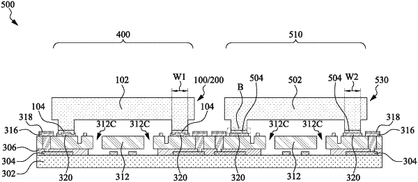
providing a device substrate comprising a plurality of semiconductor devices, wherein each of the semiconductor devices comprises a first bonding layer;
providing a cap substrate comprising a plurality of cap structures, wherein each of the cap structures comprises a second bonding layer, the second bonding layer having a planar surface and a first protrusion protruding from the planar surface, wherein the first protrusion has an outer sidewall flushed with an outer sidewall of the second bonding layer and an inner sidewall having a stepped profile; and
bonding the device substrate to the cap substrate by engaging the first protrusion of the second bonding layer of each of the cap structures with the corresponding first bonding layer of each of the semiconductor devices in the device substrate.
|