| CPC H01L 23/5386 (2013.01) [H01L 23/5383 (2013.01); H01L 23/66 (2013.01); H01P 3/081 (2013.01); H03H 7/0115 (2013.01); H01L 2223/6627 (2013.01)] | 20 Claims |
|
1. A semiconductor package, comprising:
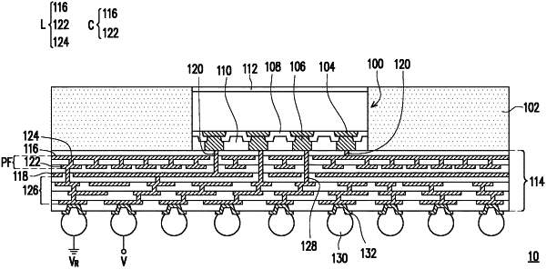
an encapsulated structure, comprising a semiconductor die and an encapsulant laterally encapsulating the semiconductor die;
electrical connectors as inputs/outputs of the semiconductor package, deployed at a front side of the encapsulated structure;
a circuit layer, lying between the encapsulated structure and the electrical connectors; and
a passive filter, embedded in the circuit layer, and comprising:
a ground plane, electrically coupled to a reference voltage;
a power plane, overlapping the ground plane, wherein a power signal is delivered to the semiconductor die through the power plane; and
conductive patches, arranged as an array between the ground plane and the power plane, and are electrically connected to the ground plane.
|